
02 / OUR CAPABILITIES
From raw silicon
to precision wafers.
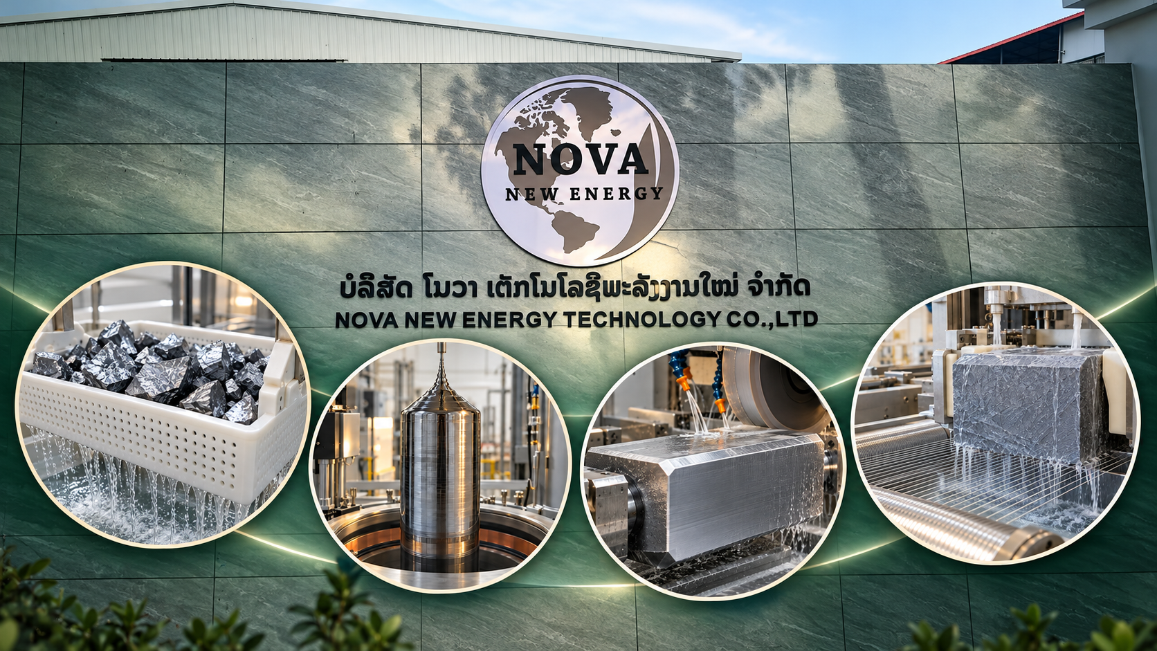

01 / PROCESS
Silicon Cleaning
Remove surface impurities. Prepare material for the next stage.
Impurity removal
Physical and chemical cleaning addresses metal-ion contamination, dust, organic residues and other surface impurities.
Controlled processing
Temperature, duration and chemical concentration are managed according to incoming material and agreed purity requirements.

02 / PROCESS
Crystal Growth
From selected polysilicon to monocrystalline ingots.
Raw-material control
High-purity feedstock selection and furnace preparation support purity throughout feeding, melting and crystallization.
Growth parameters
Temperature gradients, pulling and rotation speeds, and argon flow are controlled to support the required crystal dimensions and properties.

03 / PROCESS
Precision Machining
Shape and prepare ingots for wafer production.
Ingot preparation
Squaring and machining prepare silicon ingots for downstream bonding and slicing.
Connected production records
Every squared ingot remains connected to its upstream material records and subsequent wafer production.

04 / PROCESS
Wafer Slicing
Precision cutting for consistent wafer geometry.
Diamond-wire technology
Diamond-wire cutting and tension control support thickness consistency, surface quality and efficient use of silicon.
Process and inspection
Wire speed, feed rate and cutting conditions are monitored, with attention to thickness deviation and edge integrity.
TAILORED TO YOUR REQUIREMENTS
Individual stages.
Integrated solutions.
Cleaning plans can be adapted to material type and contamination level. Crystal growth and slicing specifications can be discussed around ingot geometry, wafer size, thickness and downstream needs. Contact our team to agree a suitable processing scope.
Discuss contract processing ↗INSIDE NOVA
Real production.
Seen up close.
A view inside our production process, from silicon material handling to the slicing workshop. Explore four short films recorded on site.
Select a film, then press play. Videos are presented without sound.